How changes in PCB fabrication are shaping innovation
Advanced PCB Technologies Introductions
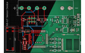
The industry of printed circuit board (pcb) fabrication is going through a revolution for more efficient, compact and high-performance electronics. These improvements do not only increase what electronic devices can do — but also promise massive sustainability and production speed advancements in PCB fabrication.
What is Laser Direct Imaging (LDI) Technology?
One of the most important innovations in PCB fabrication is Laser Direct Imaging (LDI) technology. LDI is taking over from the traditional photolithography, which involves lasers to define circuitry within a printed hard PCB. The result is increased accuracy and enables the development of boards with smaller lines, more densely package chips and reduced tolerances. For example, the technique can routinely produce line widths of 75µm in thickness (approximately half that produced by other traditional methods) when some processes struggled to get below 100µm. This capability is critical to the manufacturing of compact, lightweight boards that are essential for smartphones and medical devices.
Additive Manufacturing; 3D Printed PCB's
How 3D Printing is Changing the Way PCBs are Made This method of additive manufacturing allows for PCBs to be built layer by layer, meaning only the necessary conductive materials will be added where it is called for. Wastes are reduced with an accompanying reduction in costs as well. Some 3D Printers are capable of a resolution as fine as 10 microns, allowing for the creation of extremely minute detail. Additionally, it enables in-process material integration so that multiple materials could be printed in the same print cycle — for example multi-material PCBs combining conductive and insulating properties without skipping a beat.
We want to use AI and Automation in PCB Designing & Testing on Android Platform.
Another transformational process in PCB manufacturing is automation, driven by Artificial intelligence (AI) By introducing novels IA algorithms to PCB design tools biggest changes are the same-day turn-around and the pre-verified, performance-optimized PCB designs. In addition, testing systems driven by AI can give feedback in real time and as an intelligent system detect potential errors early in the production process, greatly improving the PCB quality of products. Certain AI systems, for instance, can reduce testing time by as much as 50% — a figure that obviously slashes the production cycle.
The Next Wave of Integration: Embedded Components
Such components directly integrated into the PCB substrate is an emerging trend. This can take the form of embedded component technology, decreasing the amount of real estate required on board and resulting in smaller and more rugged designs. This is very useful in aerospace and automotive applications where space, weight is important. According to the company, these dense components embedded into a chip-level package can significantly improve performance of electronic devices by shortening signal path lengths and minimizing electromagnetic interference (EMI).
Sustainability & ENVIRONMENTAL IMPACT.
This has made sustainability very important in PCB manufacturing. New developments are, for example, the use of lead-free solders and water-based chemicals for etching and cleaning [3]—both engineered to reduce the environmental impact of PCB production. These adjustments adhere to world regulations and also increase the security of the work environment, lowering hazardous waste. Manufactures may reduce hazardous waste by as little as about 20% to up to a reported 40%.
Conclusion
With the continuing evolution of electronics, new technologies in PCB fabrication are reaching unprecedented levels of efficiency, performance, and environmental sustainability. Every new technological push is another thing we can pat ourselves on the back for whether it truly represents progress in electronic design and manufacturing or if it brings closer to a perpetually sustainable reality with improved capabilities. Check pcb fabrication for pricing and other options in custom PCB solutions.
Besides, these advancements are equally important not only in pushing the boundaries of electronics but to also prepare the industry to sustainably and efficiently meet the needs of tomorrow.